
Home ≫ PCB Manufacturing ≫ High-speed PCB
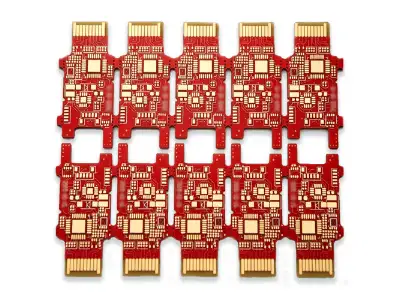
High-Speed PCB Manufacturer
We manufacture high-speed PCBs with controlled impedance and low-loss materials — built for data centers, AI servers, and next-generation network infrastructure, where every via, trace, and layer transition either preserves your signal or costs you margin.
Table of Contents
What is a high-speed PCB?
A high-speed printed circuit board is designed to maintain signal integrity for high-frequency digital signals — typically above 1 Gbps and increasingly running at 25G, 56G, or 112G per lane — using controlled impedance, low-loss laminates, and careful via and routing design to minimize signal degradation.
Unlike a standard digital board, high-speed printed circuit boards treat every trace length, via transition, and layer stackup decision as a signal-integrity variable, not just a routing convenience. For the full picture of when a design actually needs high-speed construction, see What Is a High-Speed PCB and Why It Matters.
Why Manufacturers Choose Us for high-speed boards?
- ISO 9001, UL & IATF 16949 (automotive) certified facilities
- Low-loss laminate processing (Megtron 6/7, Tachyon, and equivalents) in-house
- Backdrilling and via-stub management for 25G/56G/112G signal designs
- Engineering support from stackup design through TDR/insertion-loss verification
High-speed board Manufacturing Capabilities
| Parameter | Typical Range |
| Supported signal rates | 25G / 56G / 112G per lane |
| Base material | Megtron 6/7, Tachyon, and other low-loss laminates |
| Impedance control tolerance | ±10% |
| Layer count | Determined by stackup design |
| Backdrilling | Supported — via stub management for multi-Gbps signals |
| Minimum trace/space | 3mil / 3mil |
| Surface finish | ENIG / Immersion Silver / OSP |
| Typical lead time | 7 – 18 Days |
For how material and stackup choices affect cost and lead time, see High-Speed PCB Cost Factors Explained and the general PCB cost drivers guide.
For material selection logic beyond what’s summarized here, see High-Speed PCB Material Selection: Low-Loss Laminates and our sitewide base materials capability page.
Surface finish and impedance detail beyond high-speed-specific needs is covered in High-Speed PCB Surface Finish for Signal Performance, our sitewide surface finish options.
High-speed designs applications
High-speed signal integrity requirements show up wherever data rates climb — below are the industries we serve most, with the specific high-speed use case each one drives.
| Industry | Typical high-speed use case | Industry page |
| Datacom | Data center servers, switches, and 800G optical modules | Datacom PCB manufacturing |
| Telecom | Network backbone and switching equipment | Telecom PCB manufacturing |
| Automotive | Infotainment systems and high-speed automotive data links | Automotive PCB manufacturing |
| Medical | High-speed imaging systems | Medical device PCB applications |
| Industrial | Automation networks and industrial data backbones | Industrial PCB manufacturing |
| Safety-critical | High-speed communication systems | Safety-critical PCB manufacturing |
| Aerospace | Avionics data systems | Aerospace PCB manufacturing |
Specialized High-Speed Solutions
Data Center Switch PCB
High-speed printed circuit boards for data center switching and networking equipment, where insertion loss, crosstalk, and via-stub management directly determine whether a 56G or 112G link closes its eye diagram.
- High-Speed Signal Integrity PCB: From Data Centers to ADAS
- Data Center Switch PCB Signal Integrity Design
- High-Speed PCB for Data Center Servers
- High-Speed PCB for Network Switching Equipment
- High-Speed PCB for 800G Optical Modules
Data center switch PCB manufacturing→
Automotive Radar PCB
Automotive radar PCBs for 76–81 GHz MIMO imaging systems, where insertion loss, channel-to-channel isolation, and via-stub management directly determine whether the radar front-end closes its link budget with enough SNR to reliably detect and resolve targets at the maximum range required by NCAP and L3+ autonomous driving.
- Automotive Radar PCB Signal Integrity Considerations
Automotive radar PCB manufacturing→
Manufacturing & Process Capabilities
Differential pair routing
Length-matched, controlled-impedance differential pairs for high-speed serial links. See High-Speed PCB Differential Pair Routing Guidelines.
Via stub effects & backdrilling
Controlled-depth backdrilling to remove unused via stubs that degrade signal integrity at multi-Gbps rates. See High-Speed PCB Via Stub Effects and Backdrilling.
Impedance control
Design-stage modeling through final verification for single-ended and differential impedance. See our sitewide impedance control capability page, plus High-Speed PCB Impedance Control Requirements.
Crosstalk reduction & layer stackup
Routing and stackup techniques that keep adjacent high-speed traces from interfering with each other. See High-Speed PCB Crosstalk Reduction Techniques.
Testing & verification
TDR and insertion-loss measurement to confirm the board performs as designed before it ships. See High-Speed PCB Testing: TDR and Insertion Loss Measurement.
High-Speed board vs RF PCB
These two product lines are easy to confuse because both are built around signal integrity — the difference is what kind of signal each one is optimized for.
High-speed printed circuit board design is primarily concerned with digital signal integrity at high data rates — multi-gigabit serial links, DDR memory, PCIe, and similar buses — where timing, crosstalk, and controlled impedance across a digital channel are the dominant concerns.
RF PCB design is concerned with analog high-frequency signals — continuous-wave or modulated RF carriers — where dielectric constant (Dk), loss tangent (Df), and electromagnetic behavior at the material level matter most.
Some designs, like automotive radar, genuinely need both disciplines at once, which is exactly why our Automotive Radar PCB draws content from both this hub and our RF PCB manufacturer page.
Certified High-Speed Manufacturing
Every high-speed board we produce runs through the same quality system that governs our full product line, plus signal-integrity-specific process controls.
See our certifications page for current UL, ISO 9001, and IATF 16949 (automotive) certificates, along with our quality inspection process — and High-Speed PCB Quality Control Process for high-speed-specific detail.
What you want to ask
Frequently Asked Questions
Q: What signal speeds can your high-speed PCB manufacturing support?
A: We manufacture high-speed PCBs supporting 25G, 56G, and 112G signal rates per lane, with stackup design tailored to the target data rate — see High-Speed PCB Layer Stackup for 25G/56G/112G Signals for how stackup choices change as speeds increase.
Q: What materials do you use for low-loss high-speed PCB designs?
A: We work primarily with Megtron 6/7 and Tachyon low-loss laminates, selected based on your target signal rate, channel length, and budget. See High-Speed PCB Base Material: Megtron vs Tachyon Comparison for the detailed material comparison.
Q: Do you offer backdrilling for high-speed PCB manufacturing?
A: Yes — backdrilling is a standard part of our high-speed fabrication process, used to remove unused via stubs that would otherwise degrade signal integrity at multi-Gbps rates.
Q: What is the difference between high-speed PCB and RF PCB?
A: High-speed PCB design focuses on digital signal integrity at high data rates — timing, crosstalk, and impedance control across a digital bus. RF PCB design focuses on analog high-frequency signals, where material-level properties like dielectric constant and loss tangent matter most.
Further Reading
- AI Server PCB Design Considerations
Contact us
Ready to move forward with your high-speed PCB project?
Send us your specs, target signal rate, and material preference, and we’ll get back to you with a quote and a manufacturability review.