
Home ≫ PCB Manufacturing ≫ Heavy Copper PCB
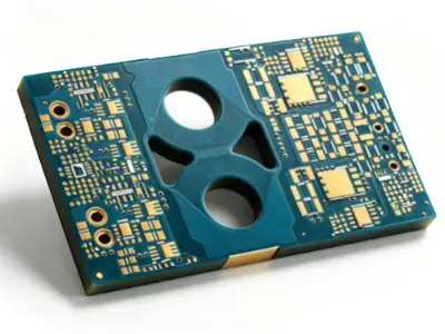
Heavy Copper PCB Manufacturer
We manufacture heavy copper PCBs from 2oz to 6oz copper weight — engineered for high-current, high-power applications in EV, energy storage, and industrial power electronics, where the copper itself has to do as much work as the circuit design.
Table of Contents
What is a heavy copper PCB?
A heavy copper board uses copper layers thicker than a standard board — typically 3oz per layer or more, up to 20oz or beyond for the most demanding designs — to carry higher current loads and dissipate heat more effectively than standard copper weights allow. That extra copper mass changes more than just current capacity: it affects etching tolerances, plating process, thermal behavior, and how the board needs to be designed from the layout stage onward.
Heavy copper construction shows up most often in power electronics, EV systems, and energy storage applications, where the board has to move real current rather than just carry a signal. For the full breakdown of when this construction is actually needed, see our guide on what a heavy copper PCB is and when to use it.
Why Manufacturers Choose Us for Heavy Copper PCB?
- ISO 9001 & IATF 16949 certified facilities
- 2 oz to 6 oz copper weight, including mixed copper weight stackups
- In-house current-carrying capacity engineering support
- From DFM review through etching, plating, and final inspection
Heavy Copper Board Manufacturing Capabilities
| Parameter | Typical Range |
| Copper weight | 2 oz – 6 oz |
| Layer count | Application-dependent — from simple 2-layer power boards to complex multilayer power/control hybrids |
| Current carrying capacity | Depends on copper weight and trace width — see calculation guide below |
| Board thickness | 0.2mm – 10mm |
| Minimum trace/space (at heavy copper weight) | 2mil/2mil |
| Surface finish | ENIG / Immersion Tin / OSP |
| Base material | Standard FR4, High-Tg FR4 for thermal-demanding designs |
| Typical lead time | 7 – 18 Days — prototype vs. production |
For a full worked methodology, see Heavy Copper PCB Current Carrying Capacity Calculation. If your project’s surface finish, base material, or thermal requirements go beyond what’s in the table above, our surface finish options, base material selection (including our High-Tg PCB guide), and PCB cost drivers capability pages cover the full range we support across all product lines.
Heavy Copper Applications
Heavy copper construction is specified wherever a board has to carry meaningful current, not just a signal. Below are the industries we serve most often, with the specific heavy copper use case each one drives.
| Industry | Typical heavy copper use case | Industry page |
| Power & Energy | Solar inverters, energy storage system controllers | Power & Energy PCB manufacturing |
| Automotive | EV powertrain electronics, EV charging systems | Automotive PCB manufacturing |
| Industrial | High-power industrial power electronics | Industrial PCB manufacturing |
| Railway | Traction system power electronics | Railway PCB manufacturing |
| Aerospace | Onboard power distribution systems | Aerospace PCB manufacturing |
Specialized Heavy Copper Solutions
Automotive Radar-adjacent note
Automotive Radar PCB is a shared RF/High-Speed vertical, not a Heavy Copper vertical — see the High-Frequency PCB manufacturing services for that page.
AI Server PCB
AI server power delivery is a heavy copper problem as much as a high-speed signal problem — this page covers the power-electronics side of AI server board design, while our High-speed PCB manufacturing services hub covers the signal-integrity side of the same application.
Explore AI server PCB manufacturing ≫
New Energy & ESS PCB
New energy vehicle and energy storage system electronics need the current-carrying capacity heavy copper provides, layered on top of the routing complexity a multilayer stackup handles. This page is the home for that combination.
Explore new energy PCB manufacturing ≫
EV Charging PCB
Charging infrastructure — from onboard chargers to charging pile power electronics — is a dedicated heavy copper use case with its own thermal and current-density considerations.
Explore EV charging PCB manufacturing ≫
BESS PCB
Grid-scale and commercial battery energy storage systems demand some of the highest current-carrying and thermal-safety requirements in power electronics.
Explore battery energy storage PCB manufacturing ≫
Solar Inverter PCB
Solar inverter and charge-controller electronics need heavy copper layouts to handle DC-to-AC conversion current without excessive heat buildup.
Explore solar inverter PCB manufacturing ≫
High-current PCB Process Capabilities
Current-carrying capacity calculation
Matching copper weight and trace width to your actual current load, not just a rule of thumb.
Etching & plating process control
Heavy copper etching behaves differently than standard copper weights, and plating has to keep pace across dramatically different feature sizes on the same board. See Heavy Copper PCB Etching Process Challenges and Heavy Copper PCB Plating Process Explained.
Mixed copper weight design
Combining heavy copper power planes with standard-weight signal layers in a single stackup. See Heavy Copper PCB Mixed Copper Weight Design.
Thermal management
Copper mass changes how heat moves through the board; see Heavy Copper PCB Thermal Management Techniques.
Heavy Copper PCB vs Standard PCB: Key Differences
The difference isn’t just copper thickness — it changes the manufacturing process itself. A standard PCB (typically 1–2oz copper) is optimized for signal routing at manageable current levels, with etching and plating tuned for fine-pitch features.
A heavy copper PCB at 3oz or above trades some of that fine-feature precision for current-carrying capacity and heat dissipation, which means different etching compensation, different plating times, and often different trace-to-trace clearance rules.
If your board is carrying meaningful current — power distribution, motor drives, charging systems, battery management — heavy copper is usually the right call; if it’s primarily routing signals, a standard or Multilayer PCB manufacturing service is more cost-effective.
Full comparison: Heavy Copper PCB vs Standard PCB: Key Differences.
Certified Heavy Copper Manufacturing
Every heavy copper board we produce runs through the same quality system that governs our full product line, plus the additional inspection heavy copper etching and plating require. See our certifications page for current ISO 9001 and IATF 16949 (automotive) certificates, as well as our quality inspection process.
What you want to ask
FAQ
Q: What copper weights can you manufacture for heavy copper PCB?
A: We manufacture heavy copper PCBs from 2 oz up through 6 oz copper weight per layer, including mixed copper weight stackups that combine heavy copper power planes with standard-weight signal layers. See Heavy Copper PCB Copper Weight Options: 3oz to 20oz for guidance on choosing the right weight for your current load.
Q: What applications require heavy copper PCB technology? A PCB suitable for flight control systems?
A: Heavy copper is specified wherever a board carries significant current or needs to dissipate heat efficiently — EV powertrain and charging systems, solar inverters, battery energy storage systems, industrial power electronics, and motor drive controllers are the most common applications we manufacture for.
Q: Can you manufacture high-current PCBs for EV and energy storage systems?
A: Yes. We manufacture high-current PCBs for EV powertrain electronics, EV charging infrastructure, and battery energy storage systems, with the current-carrying capacity and thermal design these applications demand. See our dedicated new energy PCB manufacturing and EV charging PCB manufacturing pages for application-specific detail.
Q: How is current carrying capacity calculated for heavy copper board?
A: Current carrying capacity depends on copper weight, trace width, allowable temperature rise, and whether the trace is on an internal or external layer — it’s not a single fixed number per copper weight. Our engineering team calculates this per project during DFM review; for the underlying methodology, see Heavy Copper PCB Current Carrying Capacity Calculation.
Further Reading
- Heavy Copper PCB for New Energy Vehicle Applications
- Battery Management System PCB Design Guide
- Vertical application (bridges to New Energy & ESS vertical)
- Power PCB: Why It Matters for AI Servers and New Energy Systems
Contact us
Ready to move forward with your high-current PCB project?
Send us your current-load requirements and target application, and we’ll get back to you with a copper weight recommendation, a quote, and a manufacturability review.