
Home ≫ PCB Manufacturing ≫ High-Frequency / RF PCB
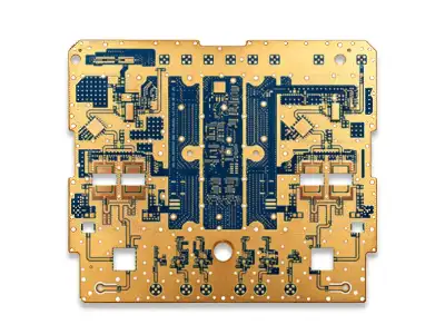
High-Frequency / RF PCB Manufacturer
We manufacture RF and radio-frequency PCBs on PTFE, Rogers, and hybrid dielectric stackups — engineered for the signal integrity that 5G, radar, and satellite communication systems depend on, where every mil of trace geometry and every layer of dielectric affects performance.
Table of Contents
What is an RF PCB?
An RF (radio frequency) PCB is a circuit board built and manufactured specifically to carry high-frequency signals — typically anywhere from a few hundred MHz up into the mmWave range — without the signal loss, reflection, or distortion that a standard FR4 board would introduce at those frequencies.
That reliability comes from a different set of material and process choices than a standard PCB: low-loss dielectrics like PTFE or Rogers laminates, tightly controlled impedance, and copper roughness and via geometry that are all tuned for the frequencies involved.
If you’re not yet sure whether your design needs true RF construction or can run on a conventional board, our guide on what an RF PCB is and how it differs from a standard PCB walks through that decision.
Why choose us to make high-frequency PCBs?
- ISO 9001 & IATF 16949 certified facilities
- PTFE, Rogers, and mixed-dielectric hybrid stackup capability
- Tight impedance control for single-ended and differential RF traces
- Engineering support from material selection through final RF/impedance test
Technical Specifications
| Parameter | Typical Range |
| Frequency range supported | up to mmWave (70 GHz+) |
| Layer count | 2–20+ layers, including mixed dielectric/hybrid stackups |
| Base material | PTFE, Rogers (4350B, 4003C, RO4000 series), hybrid PTFE-FR4 constructions |
| Dielectric constant (Dk) range | 2.2~3.5 |
| Copper roughness options | Standard/low-profile / reverse-treated (RTF) copper foil |
| Minimum trace/space | 3mil / 3mil |
| Impedance Control | ±5–10% |
| Surface finish | ENIG / Immersion Silver / OSP |
| Via structure | Through-hole, blind/buried via, via-in-pad |
| Typical lead time | 7 – 18 Days — prototype vs. production |
For a deeper look at how material choice and dielectric constant affect your quote, see RF PCB Base Material: Rogers 4350B vs 4003C Comparison.
If your project’s surface finish, base material, or impedance requirements go beyond what’s in the table above, our surface finish options and base material selection capability pages cover the full range we support across all product lines.
Radio-frequency PCB Applications
RF construction is specified wherever a design has to move signal reliably at frequency — not just at DC or low-speed digital rates. Below are the industries we serve most often, with the specific RF use case each one drives.
| Industry | Typical use case | Industry page |
| Telecom | 5G base station and small-cell RF front ends | Telecom PCB manufacturing |
| Aerospace | Satellite communication and radar systems | Aerospace PCB manufacturing |
| Automotive | ADAS and automotive radar sensor modules | Automotive PCB manufacturing |
| Medical | RF-enabled diagnostic and imaging equipment | Medical device PCB applications |
| Industrial | Industrial wireless, GPS, and IoT RF modules | Industrial PCB manufacturing |
| Safety-critical | Monitoring communication and mission-critical RF links | Safety-critical PCB manufacturing |
Specialized RF Solutions
Automotive Radar PCB
ADAS radar sensors run at frequencies and tolerances that push RF manufacturing harder than almost any other automotive electronics category. If your project is a radar sensor board, this is the resource built specifically for it.
5G Base Station PCB
5G infrastructure — from small cells to full base stations — depends on RF PCBs that hold tight impedance and low loss at frequencies conventional boards can’t support. This page collects everything specific to 5G base station RF design and fabrication.
Satellite Communication PCB
Satellite communication systems combine RF performance requirements with the reliability standards of aerospace electronics. This page is built for engineers sourcing PCBs for satellite terminals, ground stations, and onboard communication payloads.
Radio-frequency PCB Process Capabilities
Impedance control for RF signal integrity
Tight-tolerance single-ended and differential impedance across mixed dielectric stackups. See RF PCB Impedance Control for Signal Integrity.
Dielectric constant & loss tangent management
Material selection and stackup design tuned to your frequency range. Read RF PCB Dielectric Constant and Loss Tangent Explained.
Copper roughness control
Surface treatment selection to minimize insertion loss at high frequency. See RF PCB Copper Roughness and Signal Loss.
Mixed dielectric/hybrid stackup design
Combining PTFE, Rogers, and FR4 layers in a single board where cost and performance both matter. Detailed in RF PCB Mixed Dielectric Stackup Design
Via design for high-frequency signals
Via geometry and placement tuned to minimize discontinuities at frequency. See RF PCB Via Design for High-Frequency Signals.
Grounding & shielding
Layout and stackup techniques to control EMI in dense RF designs. Read RF PCB Grounding and Shielding Techniques.
RF testing & signal integrity verification
See our process in RF PCB Testing and Signal Integrity Verification.
High-frequency board vs Standard Multilayer PCB
Not every design that runs at elevated frequency needs true RF construction — and RF materials add cost that isn’t worth paying if your signals don’t demand it. The dividing line is usually frequency and signal-loss tolerance. If your board is carrying signals into the hundreds of MHz or GHz range and can’t tolerate the loss and reflection that FR4 introduces at those frequencies, RF construction on PTFE or Rogers laminate is the right call. If your design sits well below that threshold, a standard Multilayer PCB manufacturing services is almost always the more cost-effective choice, and our HDI PCB manufacturing services line covers the separate case where the driving constraint is board size and via density rather than frequency.
For the specific decision framework, see What an RF PCB Is and How It Differs From Standard PCB.
Certified RF Manufacturing
Every RF board we produce runs through the same quality system that governs our full product line, plus RF-specific test and verification steps for impedance and signal integrity. See our certifications page for current ISO 9001 and IATF 16949 (automotive) certificates, as well as our quality inspection process.
What you want to ask
FAQ
Q: What is the difference between an RF PCB and a standard PCB?
A: An RF PCB is built on low-loss dielectric materials — typically PTFE or Rogers laminates rather than standard FR4 — with tighter impedance control, controlled copper roughness, and via geometry specifically designed to minimize signal loss and reflection at high frequency. A standard PCB is optimized for cost and general-purpose digital signals, not for maintaining signal integrity into the GHz range.
Q: What frequency range can you manufacture RF PCBs for?
A: 500MHz~77GHz. Material and stackup selection both shift as frequency increases, especially heading into the mmWave range used by 5G and some radar systems — see our 5G base station PCB manufacturing page for frequency-specific detail.
Q: What base materials do you use for RF PCB manufacturing?
A: We work with PTFE, Rogers laminates (including the 4350B and 4003C families), and hybrid stackups that combine PTFE or Rogers layers with FR4 to manage cost on multilayer RF designs. See RF PCB Material Selection: PTFE vs Rogers vs FR4 for a full comparison.
Q: Do you manufacture RF PCBs for automotive radar and aerospace applications?
A: Yes. We manufacture RF PCBs for automotive radar sensor modules, aerospace radar systems, and satellite communication payloads, with the tighter tolerances and testing those applications require. See our dedicated automotive radar PCB manufacturing and satellite communication PCB manufacturing pages for application-specific detail.
Further Reading
- What Is an RF PCB and How It Differs From a Standard PCB
- RF PCB Design Challenges in 5G Systems
- 5G PCB Manufacturing: RF Design and Fabrication Considerations
- RF PCB Cost Factors: Material vs Process
Contact us
Ready to move forward with your radio-frequency PCB project?
Send us your specs — including frequency range and target application — and we’ll get back to you with a material recommendation, a quote, and a manufacturability review.