
Home ≫ PCB Manufacturing ≫ Multilayer PCB
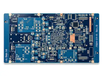
Multilayer PCB Manufacturer
From 4-layer boards to complex 60+ layer stackups, we manufacture multilayer PCBs for demanding industrial, railway, and safety-critical systems — engineered for reliability where failure is not an option.
Table of Contents
What is a multi-layer PCB?
A multilayer PCB is a printed circuit board built from three or more conductive copper layers, separated by insulating dielectric material and laminated together under heat and pressure into a single rigid structure. Compared to single- or double-sided boards, this layered construction allows for much denser routing, controlled impedance, and the integration of power, ground, and signal planes — making multilayer PCBs the standard choice for complex electronics where board space is limited and reliability requirements are high.
Why choose us to manufacture multilayer boards?
- IPC Class 2 & Class 3 Manufacturing
- 4 to 60+ Layers
- ISO 9001 / IATF 16949 Certified
- On-Time Delivery for Prototype & Production Runs
Multi-layer PCB Technical Specifications
| Parameter | Typical Range |
| Layer count | 4 – 60+ layers |
| Board Thickness | 0.8 mm – 6.4 mm |
| Copper Weight | 0.5 oz – 4 oz |
| Minimum Trace/Space | 3/3 mil |
| Minimum Drill Diameter | 0.15 mm |
| Base Material | FR4, High-Tg FR4, Polyimide (per project) |
| Surface Finish | ENIG / HASL (Lead-Free) / OSP / Immersion Silver |
| Impedance Control | ±10% tolerance, single-ended & differential |
| Via Structures | Through-hole, blind, buried, sequential lamination |
| Quality Standard | IPC Class 2 / IPC Class 3 |
| Typical Lead Time | 7 – 18 Days — prototype vs. production |
Need a spec that isn’t listed here? See our full PCB specification guide.
Industries We Serve
Multilayer PCBs are used across a wide range of demanding applications where board density, signal integrity, and long-term reliability all matter. We manufacture multilayer boards for:
| Industry | Typical use case | Industry page |
| Industrial | Automation control systems, PLCs, and factory sensor networks that need to run reliably around the clock. | Telecom PCB manufacturing |
| Railway | Signaling and interlocking systems built to EN 50155 and other rail-transit reliability standards. | Medical device PCB applications |
| Power & Energy | Power distribution units and grid infrastructure demanding high current-carrying capacity and thermal stability. | Automotive PCB manufacturing |
| Medical | Imaging equipment and diagnostic devices manufactured to ISO 13485 and IEC 60601 standards. | Datacom PCB manufacturing |
| Telecom | Switching and infrastructure equipment requiring dense, high-reliability interconnects. | Aerospace PCB manufacturing |
| Safety-critical | Redundant control systems where board failure is not an acceptable risk. | Industrial PCB manufacturing |
| Aerospace | Avionics systems built to withstand vibration, thermal cycling, and long service life. | Railway PCB manufacturing |
Specialized Multilayer Board Solutions
Industrial Robotics & Automation PCB
Multilayer PCBs for robotic controllers, motion-control systems, and factory automation electronics — engineered for EMI resistance and long-term duty-cycle reliability.
Industrial automation PCB manufacturing ≫
Railway Signaling & Control PCB
Railway signaling PCB manufacturing ≫
Manufacturing Capabilities
Layer Count & Stackup Design
From simple 4-layer boards to complex 20+ layer stackups with mixed dielectric materials. Read our Multilayer PCB Stackup Design Guide for engineering best practices.
Blind & Buried Via Processing
Sequential lamination and controlled-depth drilling for high-density interconnects. See Multilayer PCB Blind Via vs Through-Hole Via for how to choose the right via structure for your design.
Impedance Control
Tight-tolerance controlled impedance for high-speed and RF-adjacent signal layers. Full details in our impedance control capability page.
Multilayer PCB vs. HDI PCB
Multilayer and HDI (High Density Interconnect) PCBs are often confused, but they solve different problems. A multilayer PCB adds layer count to separate power, ground, and signal planes and support more complex circuitry — the layers are typically connected with standard through-holes or basic blind/buried vias.
An HDI PCB, by contrast, is defined by via density and miniaturization: microvias, finer trace/space, and sometimes any-layer construction, used when a design needs to shrink board size without cutting functionality — common in smartphones, wearables, and compact medical devices.
If your project needs more layers for routing complexity, power delivery, or plane separation, multilayer is usually the right starting point. If your constraint is board size rather than layer count, HDI is worth evaluating instead. → HDI PCB manufacturer
Certifications & Quality
Every multilayer PCB we manufacture is built under a documented quality system, with process control from incoming material inspection through final electrical test. See our full list of certifications, quality standards, and testing capability at → our PCB manufacturing certifications.
What you want to ask
Frequently Asked Questions
Q: How many layers can you manufacture for a multilayer PCB?
A: We manufacture multilayer PCBs from 4 layers up through 60+ layers, including complex stackups with mixed dielectric materials, blind and buried vias, and sequential lamination. Layer count is selected based on routing density, power/ground plane requirements, and impedance control needs — our engineering team can help determine the right layer count during the quoting stage.
Q: What is the difference between IPC Class 2 and Class 3 for multilayer PCB?
A: IPC Class 2 covers general-purpose electronics where high reliability is expected, but continuous operation isn’t mission-critical. IPC Class 3 is reserved for high-reliability electronics — think railway signaling, aerospace, medical, and safety-critical control systems — where extended field life and zero-defect tolerance are required. Class 3 involves tighter inspection criteria, stricter annular ring and plating requirements, and more rigorous documentation.
Q: Do you manufacture multilayer PCBs for railway and safety-critical applications?
A: Yes. We manufacture multilayer PCBs for railway signaling and control systems, industrial safety interlocks, and other safety-critical applications, built to IPC Class 3 and supported by the reliability testing these systems require. See our dedicated railway signaling PCB manufacturing page for application-specific details.
Q: What lead time should I expect for a high layer count multilayer PCB?
A: Lead time scales with layer count and complexity — a 20+ layer board with blind/buried vias and tight impedance tolerances takes longer than a standard 4-layer board. Expedite options are available for time-critical projects — contact us([email protected]) for a project-specific timeline.
Further Reading
- What Is a Multilayer PCB and How Many Layers Do You Need
- Multilayer PCB for Aerospace Avionics Systems
- Multilayer PCB Quality Standards: IPC Class 2 vs Class 3
- Multilayer PCB Cost Drivers: Layers vs Complexity
Contact us
Get a Quote for Your Multilayer PCB Project
Upload your Gerber files and BOM, or talk to our engineering team about your stackup before you finalize your design.