
Home ≫ PCB Manufacturing ≫ HDI PCB
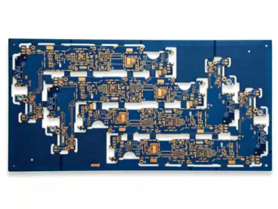
High Density Interconnect (HDI) PCB Manufacturer
We manufacture High Density Interconnect (HDI) PCBs — also known as high-density boards — with microvia, blind/buried via, and any-layer construction, engineered for compact, high-performance electronics where board space, signal density, and reliability all matter at once.
Table of Contents
What is an HDI PCB?
An HDI (High Density Interconnect) board uses microvias, finer traces, and higher connection pad density than a standard multilayer PCB, allowing designers to route far more components into a smaller footprint.
Because of that density advantage, HDI PCBs have become the default choice for 5G equipment, medical wearables, AI server modules, and other applications where every square millimeter of board real estate is at a premium.
If you’re weighing whether your design actually needs HDI construction versus a conventional board, our guide on what an HDI PCB is and when you need it walks through the decision in more detail.
Why Manufacturers Choose Us for high-density boards?
- ISO 9001 & IATF 16949 certified facilities
- Microvia, blind/buried via & any-layer HDI in-house
- 4 to 12+ layer capability, prototype through volume
- Engineering support from DFM review to final inspection
HDI Manufacturing Capabilities
| Parameter | Typical Range |
| Layer count | 4–12 layers (including any-layer construction) |
| Minimum trace/space | 2/2 mil and above |
| Microvia diameter | 0.1–0.15 mm |
| Board thickness | 0.4–3.2 mm |
| Surface finish | ENIG / OSP / Immersion Silver |
| Base material | FR4 / High-Tg FR4 / Hybrid (mixed dielectric) laminates |
| Via structure | Microvia, blind via, buried via, via-in-pad |
| Typical lead time | 7 – 18 Days |
For a deeper look at how each of these variables affects your quote, see our general PCB cost drivers guide.
If your project’s surface finish, base material, or impedance requirements go beyond what’s in the table above, our surface finish options, base material selection, and impedance control capability pages cover the full range we support across all product lines.
Applications for High-Density Interconnect Technology
HDI construction shows up wherever density, weight, and reliability requirements collide. Below are the industries we serve most often, with the specific HDI use cases each one drives.
| Industry | Typical HDI use case | Industry page |
| Telecom | 5G small cell and base station miniaturization | Telecom PCB manufacturing |
| Medical | Wearable and implantable device electronics | Medical device PCB applications |
| Automotive | ADAS camera modules, radar sensor boards | Automotive PCB manufacturing |
| Datacom | AI server and data-center switching modules | Datacom PCB manufacturing |
| Aerospace | Satellite communication modules | Aerospace PCB manufacturing |
| Industrial | IoT sensor modules, factory automation electronics | Industrial PCB manufacturing |
Specialized HDI Applications
Implantable & Wearable Medical PCB
Implantable and wearable medical devices push HDI technology to its limits: boards have to be smaller, lighter, and more reliable than almost any other application we manufacture for. If your project falls into this category, we’ve built a dedicated resource covering the manufacturing considerations specific to implantable and wearable devices.
Explore implantable medical device PCB manufacturing →
Manufacturing & Process Capabilities
HDI(microvia boards) Process Capabilities
Laser-drilled microvias down to 0.1 mm, supporting stacked and staggered via structures.
Blind & buried via construction
Sequential lamination for controlled interconnect between specific layer pairs. See our deep-dive on blind and buried via HDI PCB manufacturing.
Any-layer HDI stackups
For designs that need interconnect access from any layer to any layer, not just adjacent pairs. Compare approaches in Any-Layer HDI PCB vs Sequential Lamination.
Laser drilling capability
Read more about our laser drilling capability for HDI PCB.
Via-in-pad technology
For high-density BGA and fine-pitch component placement, see HDI PCB via-in-pad technology.
HDI vs Standard Multilayer: Which Do You Need?
Not every dense design needs HDI construction — and not every HDI-suitable design justifies the added cost. The short version: HDI makes sense when component pitch, board size, or layer-to-layer routing density genuinely require microvias; if your board has room to spare, a standard multilayer board is usually the more cost-effective choice.
For the full comparison — cost, lead time, and when each construction method wins — see our detailed guide: HDI vs Standard Multilayer PCB: Key Differences.
If your project turns out to be better suited to conventional construction, our multilayer PCB manufacturer page covers that product line in full.
Certified HDI Manufacturing
Every HDI board we produce runs through the same quality system that governs our full product line. See our certifications page for current ISO 9001 and IATF 16949 (automotive) certificates, along with our quality inspection process.
What you want to ask
FAQ
Q: What layer counts do you support for HDI?
A: We manufacture HDI boards from 4 layers up through 12+ layers, including any-layer constructions. Layer count is typically driven by component density and the number of independent signal-routing planes your design needs — see our 4-layer HDI PCB manufacturing guide and 6-layer HDI PCB stackup guide for stackup-specific detail.
Q: What is the difference between high-density boards and standard multilayer PCB?
A: HDI boards use microvias and finer trace/space geometries to pack more routing into less area, while standard multilayer boards use larger through-hole vias and are generally lower-cost for designs that don’t need that density.
Q: What industries typically require HDI PCB technology?
A: Telecom (5G infrastructure), medical devices (wearables and implantables), automotive (ADAS and radar), datacom (AI servers), aerospace (satellite communication), and industrial IoT are the industries where we see HDI specified most often — see the PCB Applications by Industry section above.
Q: What is your minimum trace and space capability for an HDI PCB?
A: 2/2 mil and above. For more on how trace/space tolerances interact with layer count and via structure, see HDI PCB Minimum Trace and Space Capability.
Other industries we serve:
Further Reading
- HDI PCB for AI Server Modules
- 4 Layer HDI PCB Manufacturing Guide
- HDI PCB Cost Factors Explained
Contact us
Ready to move forward with your high-density interconnect project?
Send us your specs, and we’ll get back to you with a quote and a manufacturability review.